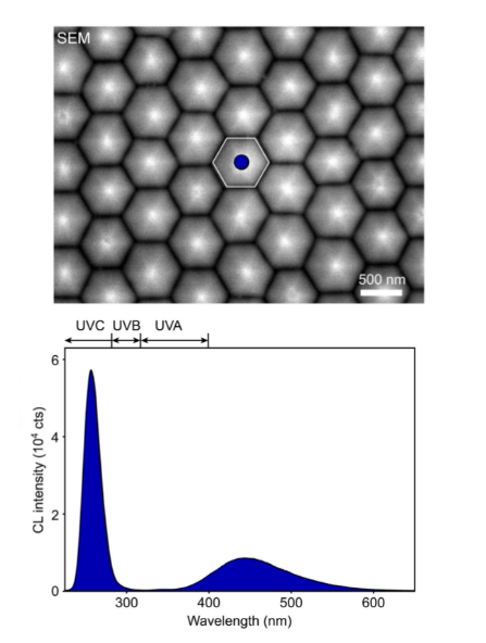
Cathodoluminescence (CL) is the emission of light from a material as a result of excitation by electrons. A variety of processes can be responsible for CL emission in different materials, and imaging CL is, therefore, a powerful technique to study them. CL imaging performed in a scanning electron microscope (SEM) is a versatile technique for the study of optical properties with deep sub-wavelength resolution. In addition to intensity mapping, advanced imaging modes such as spectroscopy, angle-resolved imaging and polarimetry, to name a few, are used to understand the physics of various materials and study device performance.
In this webinar, our Application Specialist Sangeetha Hari will focus on CL imaging for the characterization of LEDs and single-photon devices. She will give practical examples of the two applications that acquired quantitatively comparable data and characterized LEDs from the deep UV to the infrared. Join the webinar to learn how to use CL to image local defects and light emission characteristics of LEDs and single-photon devices.

